- 您现在的位置:买卖IC网 > Sheet目录2007 > LTC6900IS5#TR (Linear Technology)IC OSC SILICON 20MHZ TSOT23-5
LTC6900
9
6900fa
APPLICATIONS INFORMATION
A Ground Referenced Voltage Controlled Oscillator
The LTC6900 output frequency can also be programmed by
steering current in or out of the SET pin, as conceptually
shown in Figure 8. This technique can degrade accuracy
as the ratio of (V+ – VSET) / IRES is no longer uniquely
dependent of the value of RSET, as shown in the LTC6900
Block Diagram. This loss of accuracy will become noticeable
when the magnitude of IPROG is comparable to IRES. The
frequency variation of the LTC6900 is still monotonic.
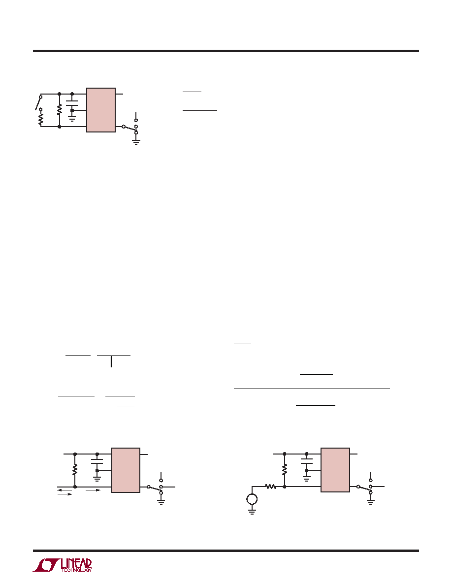
Figure 9 shows how to implement the concept shown in
Figure 8 by connecting a second resistor, RIN, between the
SET pin and a ground referenced voltage source, VIN.
For a given power supply voltage in Figure 9, the output
frequency of the LTC6900 is a function of VIN, RIN, RSET
and (V+ – VSET) = VRES:
fOSC =
10MHz
N
20k
RIN RSET
1
+
VIN V+
()
VRES
1
+
RIN
RSET
(1)
When VIN = V+, the output frequency of the LTC6900 as-
sumes the highest value and it is set by the parallel com-
bination of RIN and RSET. Also note, the output frequency,
fOSC, is independent of the value of VRES = (V+ – VSET) so
the accuracy of fOSC is within the data sheet limits.
When VIN is less than V+, and expecially when VIN ap-
proaches the ground potential, the oscillator frequency,
fOSC, assumes its lowest value and its accuracy is affected
by the change of VRES = (V+ – VSET). At 25°C VRES varies
by ±8%, assuming the variation of V+ is ±5%. The tem-
perature coefcient of VRES is 0.02%/°C.
By manipulating the algebraic relation for fOSC above, a
simple algorithm can be derived to set the values of external
resistors RSET and RIN, as shown in Figure 9.
1. Choose the desired value of the maximum oscillator
frequency, fOSC(MAX), occurring at maximum input
voltage VIN(MAX) ≤ V+.
2. Set the desired value of the minimum oscillator fre-
quency, fOSC(MIN), occurring at minimum input voltage
VIN(MIN) ≥ 0.
3. Choose VRES = 1.1 and calculate the ratio of RIN/RSET
from the following:
RIN
RSET
=
VIN(MAX) V+
() fOSC(MAX)
fOSC(MIN)
VIN(MIN) V
+
()
VRES
fOSC(MAX)
()
fOSC(MIN)
1
1
(2)
Figure 7
V+
1
2
RSET1
RSET2
3
S1
5
V+
6900 F07
4
GND
LTC6900
3V OR 5V
SET
OUT
DIV
÷10
÷100
÷1
fOSC = 10MHz
OR
()
20k
N RSET1
fOSC = 10MHz
()
20k
N RSET1//RSET2
Figure 8. Concept for Programming via Current Steering
Figure 9. Implementation of Concept Shown in Figure 8
V+
1
2
RSET
IPR
3
5
5V
V+
6900 F08
4
GND
LTC6900
0.1μF
OPEN
SET
OUT
DIV
÷10
÷100
÷1
IRES
V+
1
2
RSET
VRES
RIN
VIN
3
5
5V
V+
6900 F09
4
GND
LTC6900
0.1μF
fOSC
OPEN
SET
OUT
DIV
÷10
÷100
÷1
+
–
+
–
发布紧急采购,3分钟左右您将得到回复。
相关PDF资料
LTC6902IMS#TRPBF
IC OSC SILICON 20MHZ 10MSOP
LTC6904MPMS8#TRPBF
IC OSC SILICON 68MHZ 8MSOP
LTC6905HS5-133#TRPBF
IC OSC SILICON 133MHZ TSOT23-5
LTC6905MPS5#TRPBF
IC OSC SILICON 170MHZ TSOT23-5
LTC6906HS6#TRPBF
IC OSC SILICON 1MHZ TSOT23-6
LTC6907HS6#TRPBF
IC OSC SILICON 4MHZ TSOT23-6
LTC6908HS6-2#TRPBF
IC OSC SILICON 10MHZ TSOT23-6
LTC6909HMS#TRPBF
IC OSC SILICON 6.67MHZ 16-MSOP
相关代理商/技术参数
LTC6900IS5#TRM
功能描述:IC OSC SILICON 20MHZ TSOT23-5 RoHS:否 类别:集成电路 (IC) >> 时钟/计时 - 可编程计时器和振荡器 系列:- 产品培训模块:Lead (SnPb) Finish for COTS
Obsolescence Mitigation Program 标准包装:45 系列:- 类型:温度 - 补偿晶体振荡器(TCXO) 计数:- 频率:25MHz 电源电压:3.135 V ~ 3.465 V 电流 - 电源:1.5mA 工作温度:-40°C ~ 85°C 封装/外壳:16-SOIC(0.295",7.50mm 宽) 包装:管件 供应商设备封装:16-SOIC W 安装类型:表面贴装
LTC6900IS5#TRMPBF
功能描述:IC OSC SILICON 20MHZ TSOT23-5 RoHS:是 类别:集成电路 (IC) >> 时钟/计时 - 可编程计时器和振荡器 系列:- 标准包装:3,000 系列:- 类型:振荡器 - 晶体 计数:- 频率:- 电源电压:2.3 V ~ 5.5 V 电流 - 电源:1.07mA 工作温度:-30°C ~ 80°C 封装/外壳:SOT-665 包装:带卷 (TR) 供应商设备封装:SS迷你型-5D 安装类型:表面贴装 其它名称:AN8955SSMTXLTR
LTC6900IS5#TRPBF
功能描述:IC OSC SILICON 20MHZ TSOT23-5 RoHS:是 类别:集成电路 (IC) >> 时钟/计时 - 可编程计时器和振荡器 系列:- 产品培训模块:Lead (SnPb) Finish for COTS
Obsolescence Mitigation Program 标准包装:45 系列:- 类型:温度 - 补偿晶体振荡器(TCXO) 计数:- 频率:25MHz 电源电压:3.135 V ~ 3.465 V 电流 - 电源:1.5mA 工作温度:-40°C ~ 85°C 封装/外壳:16-SOIC(0.295",7.50mm 宽) 包装:管件 供应商设备封装:16-SOIC W 安装类型:表面贴装
LTC6900IS5TRMPBF
制造商:Linear Technology 功能描述:Resistor Set Oscillator 20MHz TSOT23-5
LTC6902
制造商:LINER 制造商全称:Linear Technology 功能描述:Multiphase Oscillator with Spread Spectrum Frequency Modulation
LTC6902CMS
功能描述:IC OSC SILICON 20MHZ 10MSOP RoHS:否 类别:集成电路 (IC) >> 时钟/计时 - 可编程计时器和振荡器 系列:- 产品培训模块:Lead (SnPb) Finish for COTS
Obsolescence Mitigation Program 标准包装:45 系列:- 类型:温度 - 补偿晶体振荡器(TCXO) 计数:- 频率:25MHz 电源电压:3.135 V ~ 3.465 V 电流 - 电源:1.5mA 工作温度:-40°C ~ 85°C 封装/外壳:16-SOIC(0.295",7.50mm 宽) 包装:管件 供应商设备封装:16-SOIC W 安装类型:表面贴装
LTC6902CMS#PBF
功能描述:IC OSC SILICON 20MHZ 10MSOP RoHS:是 类别:集成电路 (IC) >> 时钟/计时 - 可编程计时器和振荡器 系列:- 标准包装:3,000 系列:- 类型:振荡器 - 晶体 计数:- 频率:- 电源电压:2.3 V ~ 5.5 V 电流 - 电源:1.07mA 工作温度:-30°C ~ 80°C 封装/外壳:SOT-665 包装:带卷 (TR) 供应商设备封装:SS迷你型-5D 安装类型:表面贴装 其它名称:AN8955SSMTXLTR
LTC6902CMS#PBF
制造商:Linear Technology 功能描述:Programmable Oscillator IC